

Samsung Electronics unveiled its V10 Bonding V-NAND prototype with more than 400 layers and concept models for zHBM vertical stacking at the Future of Memory and Storage conference on August 4, claiming a 58 percent density jump over V9 and more than 10 times the memory density of HBM5. The world’s largest memory maker used the Santa Clara event to push wafer-bonding architecture that separates cell arrays from peripheral logic and places high-bandwidth memory directly above AI accelerators.
The moves arrive as inference workloads demand denser, cooler storage and as multi-year supply deals begin locking most of Samsung’s output for data-center customers.
More Than 400 Layers and a Wafer Bond
Samsung presented the industry-first V10 BV-NAND with 400-plus layers as the production bridge for high-capacity AI storage. Wafer bonding builds the memory cell array on one wafer and the peripheral circuitry on another optimized for logic, then joins them. That sidesteps the thermal damage high-layer etching inflicts on transistors sitting beneath the stack in conventional cell-on-peripheral designs.
The company said the result lifts memory density about 58 percent versus its V9 generation while improving read, write and input/output performance and cutting energy use. Samsung called it the dream NAND for AI. The announcement landed exactly 13 years after the firm introduced the industry’s first V-NAND at the 2013 Flash Memory Summit.
- 400-plus layers: highest disclosed Samsung V-NAND stack
- 58 percent density gain over V9
- Improved read, write and I/O speeds tuned for inference
- Lower energy consumption for high-capacity systems
Separating the cell array from the logic wafer also lets each side use process steps tuned to its own job. The array wafer can chase layer count. The logic wafer can chase transistor speed. Once bonded, the finished die carries both advantages without forcing one process recipe to serve both roles.
At the same event the firm showed its full AI portfolio, including HBM4E samples, an HBM5 model, LPDDR5X-PIM and enterprise SSDs such as the PM1763 that entered mass production in July.
Memory Climbs Straight Onto the Accelerator
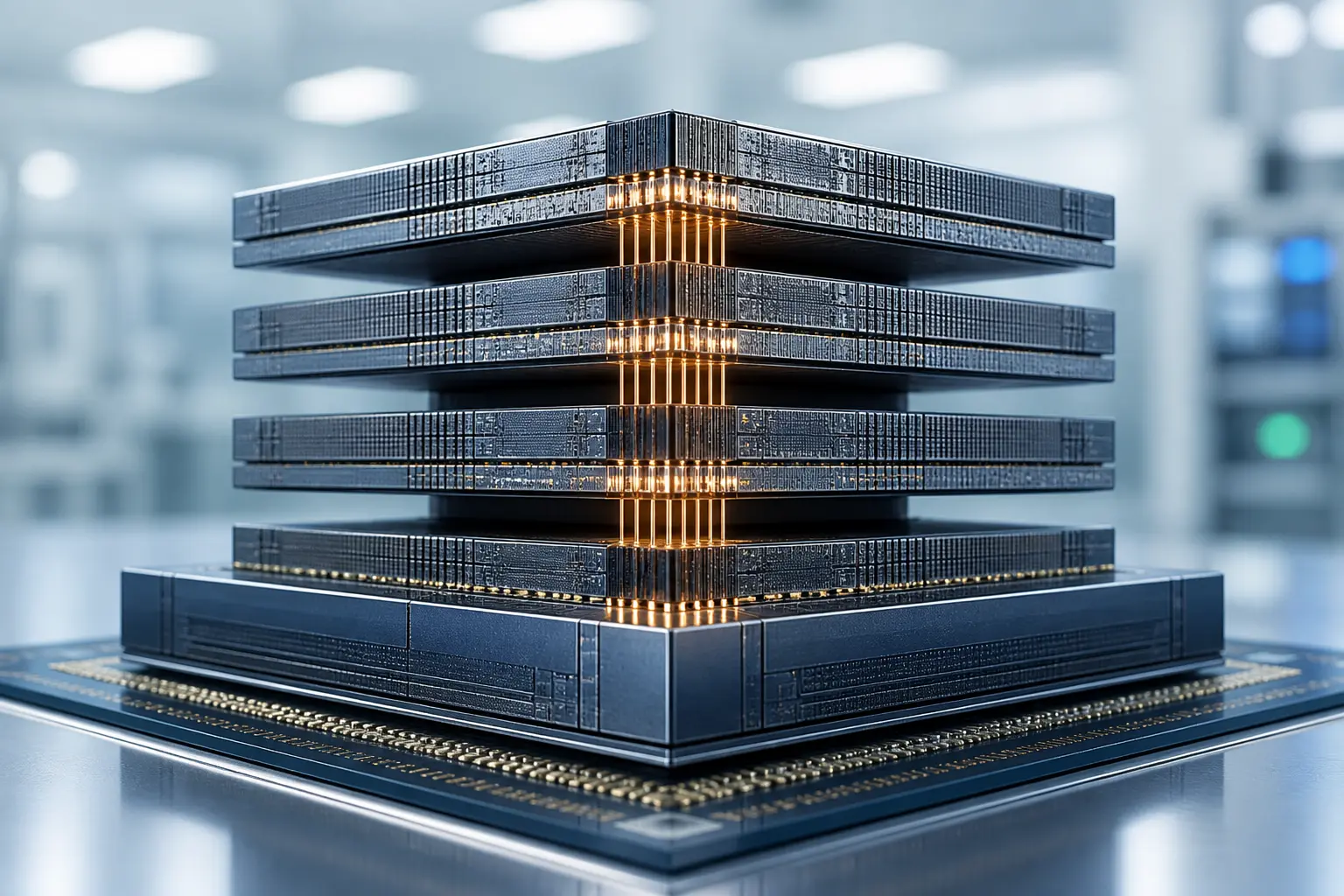
Conventional HBM sits beside the AI processor on a silicon interposer. Data travels horizontally across fine copper wiring. Samsung’s zHBM concept stacks the memory cubes vertically above the accelerator die and connects them with through-silicon vias. Distance shrinks from micrometers sideways to a direct vertical hop.
Samsung projects a next-generation interface using zHBM can deliver roughly eight times the performance of HBM5, more than 10 times HBM5 memory density, three times the energy efficiency and more than a 50 percent cut in thermal resistance. Custom intellectual property can sit in the interlayer for customer-specific caching, compression or scheduling.
| Metric | V9 NAND / HBM5 baseline | V10 BV-NAND / zHBM claim |
|---|---|---|
| NAND layers | V9 prior generation | More than 400 |
| NAND density | Baseline | +58 percent |
| HBM density | HBM5 | More than 10× |
| Energy efficiency | HBM5 | 3× |
| Thermal resistance | HBM5 | More than 50 percent lower |
| Interface performance | HBM5 | ~8× |
zHBM remains a longer-horizon concept with no commercial timeline. Thermal management of a hot accelerator bonded under memory stacks still needs solving at scale. Yet the direction is clear: memory and compute become one vertical system.
The interlayer is the flexible piece. Caching, compression or scheduling logic placed there can be tuned per customer without redesigning the memory array or the accelerator die itself. That is the commercial hook once yields and heat paths are proven.
Inference Demand Outgrew Side-by-Side Stacks
Training large models once dominated headlines. Now continuous answer generation pulls model weights, context and intermediate states from storage on every query. High-capacity NAND sits on the critical path. Side-by-side HBM still burns power and latency on horizontal hops while CoWoS-style interposer capacity stays tight, with lead times often beyond a year.
Samsung’s keynote, delivered by Jin-Yub Lee, executive vice president and head of Flash Product & Technology, and Kyungryun Kim, vice president and DRAM Design Team project leader, framed 3D structures as the answer to those bottlenecks. The firm also introduced zNAND-O, a four- and eight-layer V-NAND concept aimed at edge AI that needs low latency and high space efficiency without shipping every byte to a central data center.
The shift from training-centric to inference-centric demand changes what “good” memory looks like:
- High-capacity NAND must feed weights and context on every query, not only during training runs
- Horizontal HBM hops still cost power and add latency under continuous load
- Interposer slots remain scarce, with lead times often beyond a year
- Edge designs need compact stacks that keep data local rather than shipping every byte to a central data center
The FMS 2026 booth with roughly 30 technologies was styled like an AI cloud server to drive the point home.
Most Output Heads Into Multi-Year Contracts
Last week Samsung disclosed that long-term agreements with customers could eventually account for 60 to 70 percent of its memory sales. Five major global data-center operators have already signed; five more large AI customers sit near completion. Those deals typically include volume commitments, price floors and advance payments.
The arithmetic is simple. If 60 to 70 percent of production is reserved for AI hyperscalers, the remaining 30 to 40 percent must cover smartphones, PCs, enterprise storage and everything else. That allocation already shows up in results: the Device Solutions semiconductor division posted record profit while the Galaxy mobile division recorded its first operating loss, both shaped by capacity and pricing steered toward AI.
- 60-70 percent of memory sales potentially locked in LTAs
- Five signed hyperscale customers, five more near close
- Record semiconductor profit alongside mobile operating loss
- Inventories across DRAM and NAND still below historical levels per Citi
Buyers outside the top AI tier face tighter supply and the same recent memory price pressures hitting Samsung and Microsoft that have already rippled through the market.
Advance payments and volume floors give Samsung clearer factory planning. They also shrink the spot pool that phone, PC and general enterprise buyers once relied on. When inventories across DRAM and NAND already run below historical levels, that smaller residual slice tightens faster than the headline capacity numbers suggest.
Interposers Lose Their Monopoly
Every current HBM generation from HBM1 through the HBM5 targeted for roughly 2028 mass production relies on the silicon interposer. That substrate underpins TSMC’s CoWoS packaging, one of the most capacity-constrained links in the AI chain. zHBM makes the interposer optional for the memory-to-accelerator connection.
A next-generation interface system incorporating zHBM is expected to deliver approximately eight times the performance of HBM5. With next-generation wafer bonding technology, zHBM can achieve more than 10 times the memory density of HBM5 while enhancing energy efficiency threefold and reducing thermal resistance by more than half.
That language comes straight from Samsung’s own release. If the architecture reaches commercial yield, the packaging economics shift. Fewer horizontal traces mean less reliance on the scarcest advanced-packaging slots. Samsung, as the only major IDM spanning memory, foundry and advanced packaging, positions the stack as a one-stop turnkey path that shortens customer development cycles.
The second-order effect is structural: the firm is not merely selling denser chips. It is offering an alternative assembly model while locking the majority of its own output to the customers who need it most. Massive AI infrastructure bets already reshaping chip demand make that allocation rational for Samsung and painful for everyone else.
Bonding Puts Logic on Its Own Wafer
Conventional cell-on-peripheral NAND builds the logic first, then stacks cells above it. Each new layer of etching adds heat and process stress that the transistors underneath must survive. Past a certain height that bargain breaks down.
Wafer bonding breaks the sequence. One wafer carries only the cell array and can be pushed toward extreme layer counts. The other wafer carries only peripheral circuitry and can use a logic-friendly process. The join comes last, so the logic never endures the full etch thermal cycle.
That split is what lets V10 BV-NAND clear more than 400 layers while still claiming better read, write and I/O behavior plus lower energy use. The same bonding idea appears in the 900-layer prototype built earlier this year from two 450-layer structures with Cell Multi-Bonding, and in the multi-BV path executives have sketched toward 1,000 layers by 2030.
Kioxia’s BiCS10 already uses similar wafer bonding at 332 layers, so the technique is not unique to Samsung. The difference is how far Samsung is pushing the bonded stack as the production bridge for AI storage rather than a one-off density stunt.
Vertical Integration Meets Sideways Hierarchy
Samsung’s vertical bet is only one answer to the same inference bottleneck. Rivals at the same conference chose a different geometry: widen the memory hierarchy instead of collapsing the distance between memory and compute.
| Approach | Who | What it adds |
|---|---|---|
| Zero-distance vertical stack | Samsung zHBM / BV-NAND | Memory above the accelerator; bonded high-layer NAND |
| New mid-tier flash | SK Hynix with SanDisk | High Bandwidth Flash under an Open Compute Project standard |
| Tiered architecture | SK Hynix IMTE | Claim of roughly 36 percent better inference efficiency |
| Bonded NAND at 332 layers | Kioxia BiCS10 | Wafer bonding without the full vertical accelerator stack |
High Bandwidth Flash sits between HBM and SSDs. It gives inference engines another place to park data without paying full HBM cost or full SSD latency. IMTE extends that idea into a tiered system. Both moves assume the interposer-and-sideways model remains the default and try to make it more efficient.
Samsung assumes the opposite. Shrink the hop to a through-silicon via, put custom logic in the interlayer, and treat packaging itself as the product. The nearer-term commercial piece remains BV-NAND. zHBM is the longer bet. Which geometry wins will depend on yields, thermals and how fast customers can redesign boards around a vertical stack.
Thirteen Years After the First Vertical NAND
Samsung’s first commercial V-NAND in 2013 carried 24 layers. The progression has been relentless. V10 BV-NAND now clears 400. Earlier this year the company showed a 900-layer prototype built by bonding two 450-layer structures with Cell Multi-Bonding. Executives have sketched a multi-BV path toward 1,000 layers by 2030.
- 2013: Industry-first V-NAND, 24 layers
- 2024-25: V10 roadmap appears in trade press; 900-layer CMB prototype
- February 2026: industry-first commercial HBM4 shipment in February
- May 2026: First HBM4E samples shipped to customers
- July 2026: PM1763 PCIe Gen6 SSD enters mass production
- August 4, 2026: V10 BV-NAND prototype and zHBM/zNAND-O concepts at FMS
Rivals are not standing still. At the same conference SK Hynix detailed High Bandwidth Flash, a new tier between HBM and SSDs developed with SanDisk under an Open Compute Project standard, plus an IMTE tiered architecture claiming roughly 36 percent better inference efficiency. Kioxia’s BiCS10 uses similar wafer bonding at 332 layers. The architectural split is clear: Samsung bets on zero-distance vertical integration; others expand the memory hierarchy sideways.
Crowd reaction on X treated the vertical hop as the real break. Several posts noted that custom interlayer logic could let fewer chips handle workloads that now require multi-GPU clusters, while others flagged the molybdenum process shift and the still-unsolved thermal stack as open engineering questions. The nearer-term commercial piece remains BV-NAND; zHBM is the longer bet.
Samsung now holds both a density leap ready for production scaling and a packaging vision that could rewrite how AI accelerators talk to their memory. Whether yields and thermals cooperate will decide how fast the second-order effects hit the rest of the market.